超電導センサテクノロジー株式会社 SUSTEC(Superconducting Sensor Technology Corporation; SUSTEC)

Home > Technology > Device Fabrication
Fabrication technology
- Achieves high sensitivity and high tolerance to magnetic field with
oxide multilayer process -
We are fabricating high-temperature superconducting SQUID with a structure that cannot be realized anywhere else, making full use of oxide multilayer technology including two layers of high-temperature oxide superconductors [1]. In the single-layer process that is generally used in high-temperature superconducting SQUID, only simple and inefficient device structures can be manufactured because crossover wiring cannot be used. The multi-layered process we have developed allows the use of crossover wiring to create complex device structures that can detect magnetic fields efficiently. Due to the effect that the overhang part magnetically shields the Josephson junction, we have realized an device that can operate stably outdoors and is tolerance to the disturbance of the external magnetic field [2].
References:
[1]S. Adachi, A. Tsukamoto, T. Hato, J. Kawano, and K. Tanabe, IEICE Trans. Electron., Vol. E95-C, No.3, pp.337-345 (2012).
[2] Y. Hatsukade, et. al., “Characteristics of an HTS-SQUID gradiometer with ramp-edge Josephson junctions and its application on robot-based 3D-mobile compact SQUID NDE system”, Physica C 471 (2011) 1228.

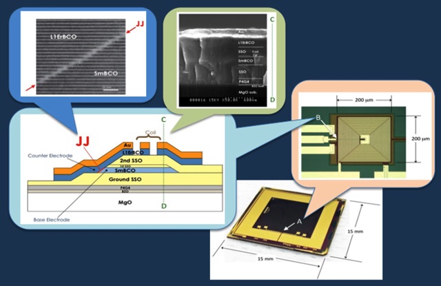
The figure above shows an example of the device structure. A total of 7 layers of oxide thin films are epitaxially grown on a magnesium oxide (MgO) single crystal substrate. The upper left is a transmission electron micrograph of the Josephson junction interface taken at the atomic image level. The period of horizontal stripes is about 1.2 nm. It can be seen that a uniform barrier layer of about 1 nm that functions as a Josephson junction is formed at the interface between the two superconducting layers. The right is an optical micrograph of the fabricated device. Signals are transmitted to SQUID with high efficiency via a spiral coil created in an area with an outer diameter of 200 μm × 200 μm.

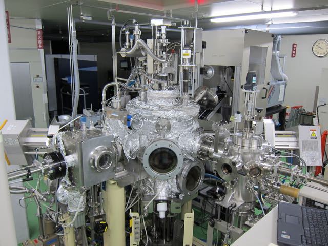
All SQUID devices are fabricated in our clean room. The upper photograph shows an off-axis sputtering machine used to fabricate the oxide layers up to the sixth layer. The 7th upper superconducting layer is made by a laser ablation method. We perform microfabrication processes using maskless direct write lithography and ion beam milling.